RESEARCH &
DEVELOPMENT
研究開発
MEMS & precision electroforming for fine processing technology.
『Fine hole processing』
Precision electroforming is an efficient technology for the mass production of precision parts that require high precision at short time and low cost.
With palladium electroforming & nickel electroforming that combines photolithography techniques and electroforming, we have realized the fine hole processing with high precision that difficult to achieve by etching process, and has been working on numerous prototype developments in various fields.
With our world-class technology, we offer a high quality plating process that meet your needs.
Features of our fine hole processing technology
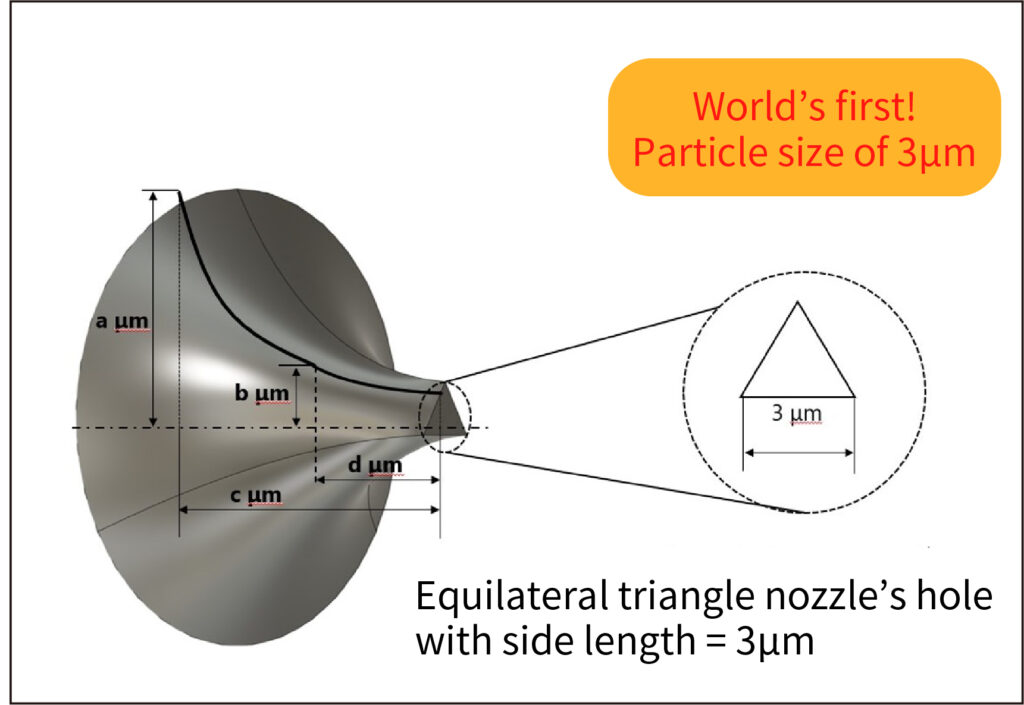
World’s first! Particle size of 3μm, fine nozzle design
We have realized the metal mesh for spray nozzle with 3μm particle size. With our original technology and know-how, we can offer you the most suitable nozzle’s hole shape for your application.
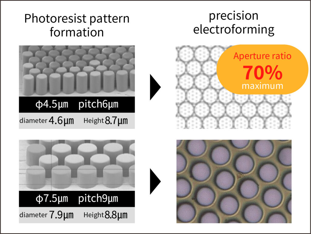
Almost all hole! Narrow pitch filter with opening ratio 70%
The minimum pitch is “resist hole diameter + 1.5㎛”. The maximum aperture ratio is 70%.
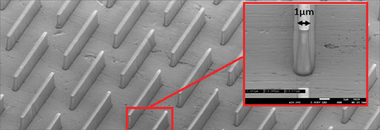
High accuracy with minimum hole diameter of 2 μm and hole diameter accuracy of ±1 μm.
Speedy, accurate and stable ultra-fine hole processing is a technique that can only be achieved by our company, which has been involved in plating for more than 100 years since our founding.
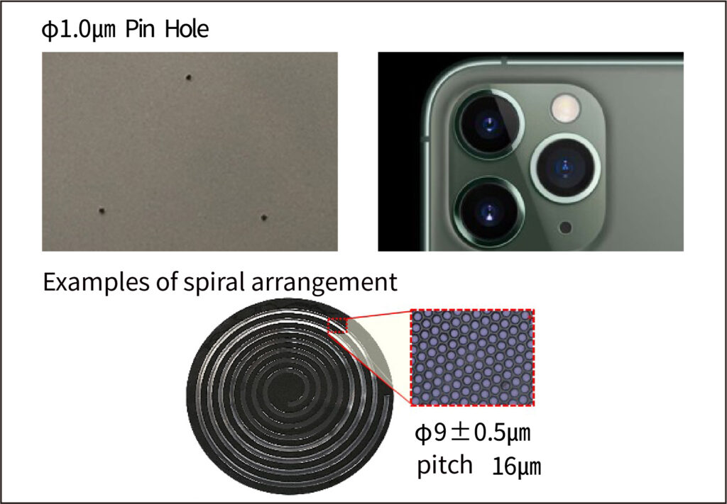
Φ1.0㎛, high-precision pinhole processing at the target location
High-precision pinhole processing of Φ1±0.2㎛ at any location.
The shape, size, and arrangement of the holes can be made as desired! The roundness is high and the edge of the hole is finished very smoothly.
Latest 3D photolithography and advanced electroforming technology
3D structure resist pattern formation process
By applying 3D photolithography, we have achieved unique 3D shaped precision electroplating.
Introduced the latest maskless laser drawing equipment and developed a new method to form micron-order three-dimensional photoresist pattern on a flat substrate.
We support the commercialization of customer’s ideal microstructures with high-precision electroforming that enables the formation of micro holes of 3 μm or less, which is impossible to achieve by machining process.
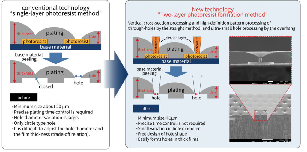
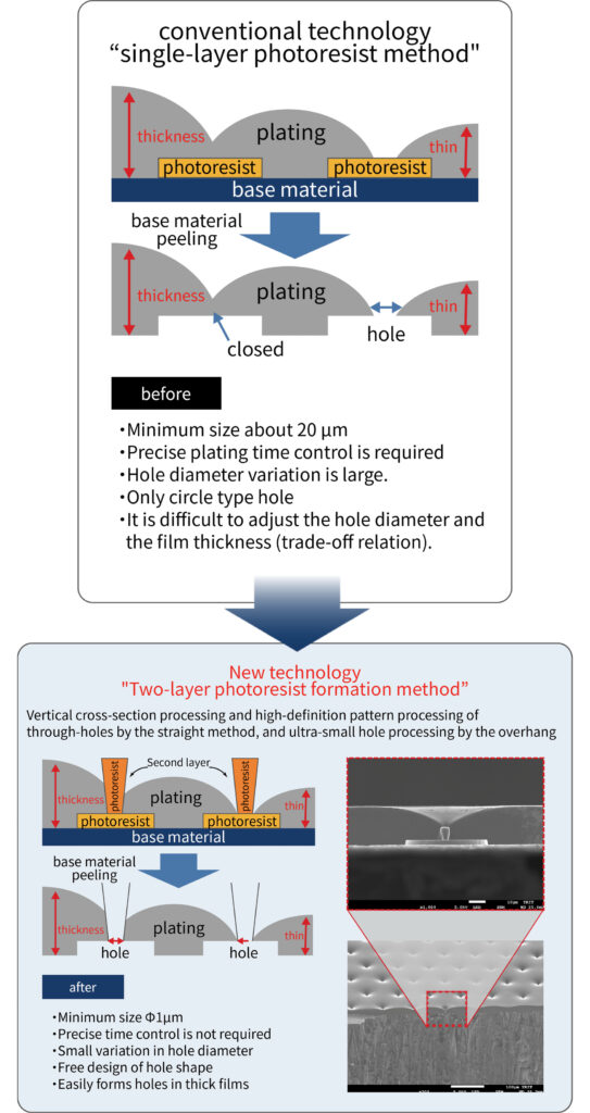
Proprietary multi-layer resist formation method
Our unique technology, multi-layer resist formation, eliminates the problems of conventional single-layer resist formation.
It is possible to form finer and more precise holes.
Variation in hole diameter within Φ8 inch wafer surface is within ±0.5㎛.
Adding functionality to fine molds
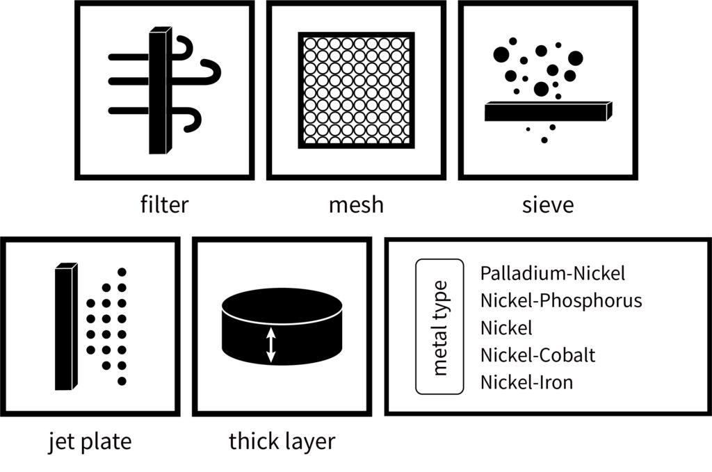
By arranging the characteristics of the electrodeposited material according to the purpose of the mold, we add functions such as corrosion resistance to the ultra-precision mold stamper.
In addition to pure nickel, which is generally used for electroplating, we also offer plating with alloys that add other metal materials to improve durability, heat resistance, and hardness.
Short-time, low-cost new manufacturing method for ultra-precision molds under development
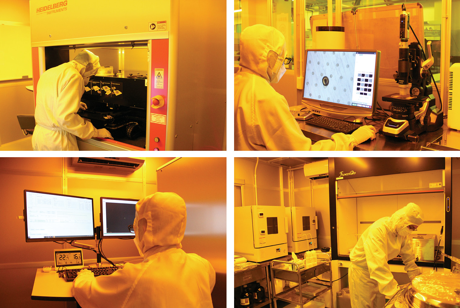
We have a FED-STD-209D class 1000 clean room for 3D photolithography. Under thorough management, we develop new technologies and new products with high precision, high quality and low cost.